Semiconductor Metrology: Key Metrics That Affect Yield


Semiconductor Metrology: Key Metrics That Affect Yield
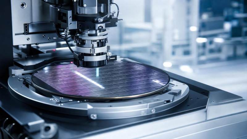
Semiconductor metrology sits at the center of yield control. It turns process variation into measurable signals before defects become expensive wafer loss.
As device nodes shrink, tolerance windows get tighter. Small shifts in dimension, alignment, thickness, or roughness can quietly reduce performance and reliability.
That is why semiconductor metrology is not just an inspection step. It is a decision system for lithography, etch, deposition, CMP, and final process qualification.
In practical fab operations, the right metrics help teams detect drift early, isolate tool issues faster, and protect cycle time. The wrong metrics create blind spots.
This matters even more during tool evaluation. A metrology platform may look strong on resolution, yet fail on throughput, repeatability, or matching across multiple chambers.
The core question is straightforward: which semiconductor metrology indicators actually affect yield, and how should they be weighed during selection and process control?
Why Semiconductor Metrology Directly Changes Yield
Yield loss rarely comes from one dramatic event. More often, it builds from small process errors that stack across hundreds of steps.
Semiconductor metrology makes those errors visible. It links physical wafer conditions to electrical outcomes, enabling tighter process windows and more reliable root cause analysis.
From a cost perspective, better measurement reduces scrap, unplanned rework, false alarms, and unnecessary maintenance. It also improves confidence in process transfers between lines or fabs.
More importantly, semiconductor metrology supports statistical process control. Without trustworthy measurement data, control charts look precise but can still drive poor decisions.
The Link Between Measurement and Decision Quality
A measurement result only matters if it changes action. Good semiconductor metrology improves feedback loops in three ways:
- It detects variation before electrical test failures appear.
- It separates process drift from tool noise.
- It supports faster parameter tuning with less trial-and-error.
That is the operational value technical teams usually care about most. Resolution alone does not guarantee better fab decisions.
Critical Dimension Variation: The First Yield Signal
Critical dimension, or CD, remains one of the most important semiconductor metrology metrics. It measures whether patterned features match target width and shape.
CD variation affects transistor behavior, resistance, capacitance, leakage, and switching speed. Even a small shift can push devices outside specification.
The more useful question is not just average CD. It is CD uniformity across the wafer, across the lot, and across repeated runs.
What To Evaluate
- Mean CD versus target specification.
- Within-wafer non-uniformity.
- Wafer-to-wafer repeatability.
- Line edge roughness and line width roughness.
- Sensitivity to resist profile and etch bias.
In advanced nodes, roughness metrics matter more than many teams expect. They can degrade variability long before mean CD moves outside control limits.
When reviewing semiconductor metrology tools, repeatability under realistic fab conditions is often the better predictor of yield impact than brochure-level resolution.
Overlay Accuracy: Alignment Errors That Quietly Destroy Margin
Overlay describes how accurately one patterned layer aligns to another. In multilayer device structures, overlay error can directly damage electrical connectivity.
This is one of the most yield-sensitive areas in semiconductor metrology. Poor overlay may not be obvious visually, yet it can cause opens, shorts, and timing failures.
As pattern density rises, the usable overlay budget becomes smaller. That makes tool matching and stage stability much more important.
Overlay Metrics That Matter
- Mean overlay error.
- Intra-field and inter-field overlay performance.
- Tool-induced shift and matching error.
- Dynamic stability over production time.
- Sensitivity to wafer warpage and topography.
A tool can produce good overlay in a controlled demo, then weaken under real thermal load and production throughput. That gap should be tested early.
For technical evaluation, semiconductor metrology performance must be reviewed at process conditions close to actual line use, not idealized samples alone.
Film Thickness and Uniformity: Hidden Drivers of Electrical Performance
Thin films define insulation, conduction, stress behavior, and interface quality. That makes thickness metrology central to both yield and long-term device reliability.
Film thickness errors influence threshold voltage, resistance, dielectric strength, and etch selectivity. Non-uniformity can amplify variation in downstream patterning steps.
The key is not just nominal thickness. Composition, refractive properties, and interface consistency can also change whether the process remains inside a safe control window.
Useful Film Metrics
- Average thickness by layer type.
- Within-wafer and across-lot uniformity.
- Refractive index or optical constant stability.
- Interfacial roughness and stack consistency.
- Repeatability after preventive maintenance or chamber clean.
Recent process changes have made multi-layer stacks harder to characterize. This means semiconductor metrology must often combine optical, X-ray, and profile-based methods.
Defect Density: The Metric With The Clearest Cost Impact
Defect density is the most direct yield metric in many lines. It measures particles, pattern defects, scratches, residues, voids, and other killer or nuisance events.
Not every defect causes electrical failure. The challenge is distinguishing critical defects from noise, then setting practical action thresholds.
That is where semiconductor metrology and inspection begin to overlap. Better classification reduces false excursions and keeps engineering attention on high-risk signals.
What To Watch Closely
- Defect count by size and type.
- Spatial distribution across wafer and lot.
- Capture rate for repeating defects.
- Classification accuracy versus manual review.
- Correlation with electrical failure bins.
A very sensitive inspection setting can overwhelm review capacity. In actual business terms, that slows response and can hide the truly expensive failures.
The better approach is to align semiconductor metrology thresholds with yield relevance, not with raw defect counts alone.
Measurement System Quality: The Metric Behind All Other Metrics
A metrology result is only trustworthy when the measurement system itself is stable. This is where many evaluations stay too shallow.
Semiconductor metrology should be judged on precision, reproducibility, matching, and long-run drift. These factors determine whether the data can support process decisions.
Core System Indicators
- Repeatability over short intervals.
- Reproducibility across tools and operators.
- Tool-to-tool matching for fleet deployment.
- Measurement uncertainty versus process window.
- Stability after calibration and over maintenance cycles.
This also connects to standards thinking. Traceability, calibration discipline, and method validation are essential when comparing suppliers or qualifying new production tools.
A simple rule helps here: if measurement uncertainty consumes too much of the process tolerance, semiconductor metrology loses practical control value.
How To Evaluate Semiconductor Metrology Tools More Effectively
A solid evaluation framework connects tool specs to yield, throughput, and integration risk. Looking at a single benchmark number is rarely enough.
- Map each metrology metric to a known yield mechanism.
- Test on realistic wafers, not only clean reference samples.
- Review repeatability across shifts and environmental changes.
- Check data integration with SPC, MES, and APC systems.
- Assess throughput against sampling strategy and cycle time.
- Compare maintenance burden, uptime, and calibration frequency.
More visible signals in recent fab upgrades show that integration speed matters almost as much as raw measurement capability. Delayed data can weaken control loops.
For supplier comparison, it helps to ask one direct question: which semiconductor metrology tool improves decision quality fastest without adding unstable complexity?
Final Takeaway
The semiconductor metrology metrics that affect yield most are CD variation, overlay accuracy, film thickness uniformity, defect density, and measurement system stability.
Each metric matters because it connects directly to process risk, electrical behavior, and production cost. None should be reviewed in isolation.
In real fab decision-making, the best semiconductor metrology approach is the one that produces accurate, actionable, and timely data under production conditions.
That is the standard worth using when selecting tools, tightening control plans, and building a more resilient path to higher yield.
Recommended for You
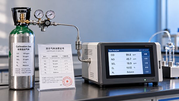
 What tolerance does a custom gas mixture need for calibration?Choose the right custom gas tolerance for calibration. Learn how blending tolerance, certified uncertainty, and stability affect accuracy—and avoid paying for precision you don’t need.
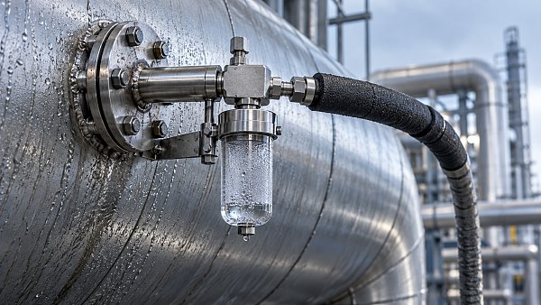
 How condensation affects stack detector readings in wet flue gasStack detector readings can drift when wet flue gas condenses. Learn how to identify moisture interference, prevent sample losses, and improve emissions monitoring reliability.
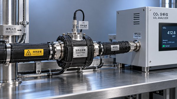
 How to prevent condensation in a CO2 analyzer sampling systemPrevent condensation in your CO2 analyzer sampling system. Learn how to control dew point, eliminate cold spots, and manage moisture for reliable readings and fewer costly disruptions.
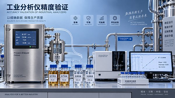
 How to verify accuracy claims for industrial quality analyzersVerify accuracy claims for industrial quality analyzers with calibration checks, independent testing, and clear acceptance criteria. Learn how to reduce risk and buy with confidence.
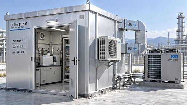
 How to calculate cooling loads for an industrial analyzer shelterSize industrial analyzer shelter cooling with confidence. Learn to calculate equipment heat, solar gains, and ventilation loads, then select HVAC capacity for reliable analyzer performance.
 How Much Does a Complete CEMS Integration Project Typically Cost?How much does a complete CEMS integration project typically cost? Explore budget ranges, hidden installation costs, and compliance needs to compare quotes and plan confidently.
 What Is the Typical Response Time for Industrial Air Monitors?What is the typical response time for industrial air monitors? Explore T90, sampling delays, and alarm settings to compare performance and choose the right monitor with confidence.
 Do Regulatory Monitoring Systems Need Third-Party Certification?Do regulatory monitoring systems need third-party certification? Learn when it is required, what certificates prove, and how to verify compliance before buying.
 How Do You Choose Wired or Wireless for Stack Monitoring?Learn how to choose between wired and wireless for stack monitoring. Compare reliability, lifecycle costs, and data recovery to find the right CEMS setup for your site.
 What Happens When Combustible Gas Sensor Calibration Is Overdue?What happens if combustible gas sensor is not recalibrated on time? Discover the risks of inaccurate readings and missed alarms, plus steps to restore reliable protection.
 Can One Multi-Gas Detector Replace Four Separate Analyzers?Find out: can a single multi-gas detector replace four separate analyzers? Compare accuracy, safety, compliance, and lifetime costs to make a confident buying decision.
 Industrial Safety vs. Emission Monitoring: What Are the Differences?What are the main differences between industrial safety and emission monitoring? Compare goals, sensors, response times, and compliance needs to choose the right systems for your facility.
 Is Remote Monitoring Worth the Cost for Small Emission Sources?Is it worth investing in remote monitoring for small emission sources? Compare costs, compliance needs, and potential savings to choose the right solution for your operation.
 How Do You Handle Analyzer Failure During an Environmental Audit?Learn how to handle analyzer failure during environmental compliance audit procedures. Protect evidence, verify data, and restore monitoring with this practical response guide.
 Do VOC Monitors Require Explosion-Proof Certification?Does VOC monitoring require explosion-proof certification? Learn when approval is needed, compare ATEX and IECEx, and choose the right monitor for your site.
 How sample conditioning affects accuracy in petrochemical analyzersImprove accuracy in petrochemical analyzers with smarter sample conditioning. Discover how phase control, filtration, and transport design prevent bias and deliver reliable process data.
 How to troubleshoot sensor drift in industrial gas detectorsIndustrial gas detectors showing sensor drift? Learn how to verify calibration gas, identify root causes, and determine when sensor replacement is needed for reliable monitoring.
 How to judge whether a competitive price reflects real valueCompetitive Price: learn how to compare scope, compliance, performance, and lifecycle costs to identify real value, reduce risk, and make smarter purchasing decisions.
 When custom gas analysis is the right fit for complex process streamsCustom gas analysis for complex process streams: learn when tailored sampling, interference control, and reliable measurement design deliver confident decisions.
 When does a laser gas analyzer meet stack emissions monitoring needs?Laser gas analyzer for stack emissions: learn when it delivers fast, reliable data, how to assess installation risks, and what to verify for CEMS compliance.
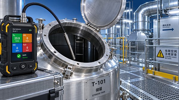
 How to select a hazardous gas analyzer for confined spacesHazardous gas analyzer selection for confined spaces: compare sensors, sampling, certifications, alarms, and maintenance to protect workers and choose with confidence.
 When is a single gas analyzer sufficient for workplace safety monitoring?Discover when a single gas analyzer delivers reliable workplace safety monitoring, and learn the key limits, calibration needs, and risks that require broader detection.
 How to choose an ambient gas analyzer for low-level leak detectionAmbient gas analyzer selection for low-level leak detection: compare sensitivity, cross-sensitivity, sampling design, alarms, and calibration for reliable site performance.
 How to tell when an oxygen sensor needs replacementOxygen sensor replacement signs explained: learn how live data, fault codes, wiring checks, and exhaust inspections pinpoint the real issue before you buy.
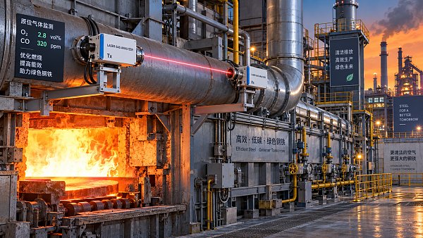
 How laser gas analyzers improve combustion control in steel furnacesLaser gas analyzer for steel industry applications delivers fast in-situ O₂ and CO data to optimize furnace combustion, cut fuel waste, and improve steel heating stability.
 How to verify whether explosion proof equipment meets site requirementsExplosion proof equipment verification made practical: match zones, gas or dust groups, temperature classes, certificates, and installation conditions for confident compliance.
 How industrial gas analysis helps detect contamination before releaseIndustrial Gas Analysis helps detect moisture, oil, oxygen, and toxic contaminants before release—protecting processes, ensuring compliance, and reducing costly risks.
 When is electrochemistry detection the right choice for water analysis?Electrochemistry detection for water analysis: learn when fast, reliable monitoring of ions, chlorine, pH, and more delivers actionable results.
 How industrial standards reduce quality risks in supplier selectionIndustrial Standard guidance helps quality and safety managers reduce supplier risks, verify compliance, strengthen traceability, and build resilient instrumentation supply chains.
 When does a multi-component system reduce installation complexity?Multi component systems reduce installation complexity when they eliminate field interfaces, streamline commissioning, and provide proven compatibility. Learn how to assess total cost and supplier accountability.
 How to size an industrial control shelter for outdoor equipmentIndustrial control shelter sizing guide: optimize layout, HVAC, access, safety, and expansion space for reliable outdoor equipment operations.
 How flue analysis helps verify combustion efficiencyFlue analysis verifies combustion efficiency by assessing O2, CO, CO2, and stack temperature to identify excess air, incomplete combustion, and heat losses.





Search Categories
Search Categories
- Smart Meters & Power Quality
- Transformer Gas Analyzers
- BESS Thermal Runaway Detectors
- Energy, Power & Smart Grid Monitoring
- Optical Profilers & CMM
- Ultrasonic & X-Ray NDT
- Calibration Standards
- Precision Metrology & NDT
- Water Quality Analyzers
- CEMS & VOCs Monitors
- Price Trends
- Import & Export Updates
- Market Trends
- Industry News
- Industry Insights
Latest Article
- What tolerance does a custom gas mixture need for calibration?Choose the right custom gas tolerance for calibration. Learn how blending tolerance, certified uncertainty, and stability affect accuracy—and avoid paying for precision you don’t need.Posted by:
- How condensation affects stack detector readings in wet flue gasStack detector readings can drift when wet flue gas condenses. Learn how to identify moisture interference, prevent sample losses, and improve emissions monitoring reliability.Posted by:
- How to prevent condensation in a CO2 analyzer sampling systemPrevent condensation in your CO2 analyzer sampling system. Learn how to control dew point, eliminate cold spots, and manage moisture for reliable readings and fewer costly disruptions.Posted by:
Please give us a message